Aolong Sun孙 奥 龙
PhD Student · Fudan University · Photonic Computing for AI
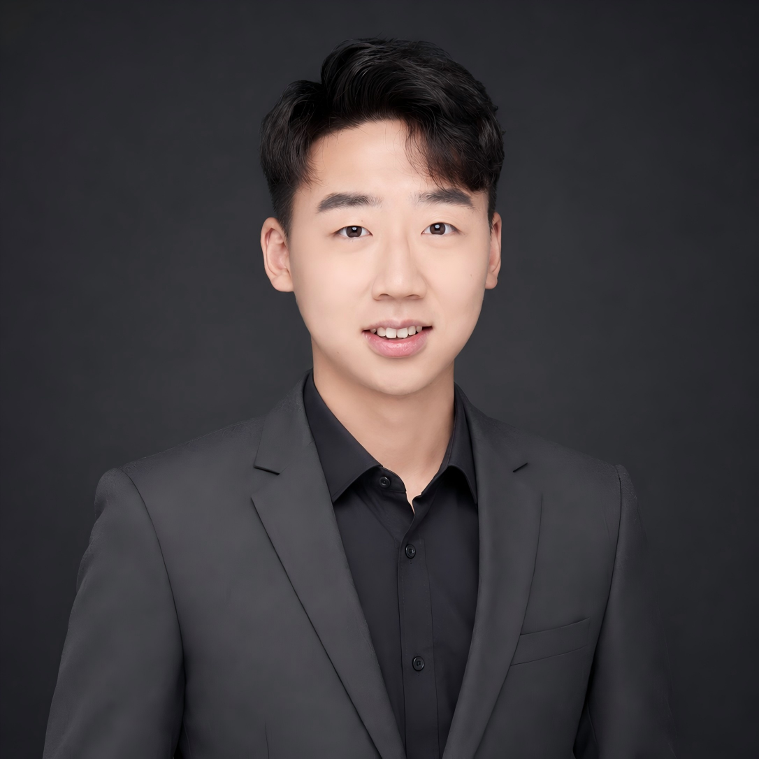
I am a PhD student at Fudan University and currently a visiting PhD researcher at the A*STAR Institute of Microelectronics (IME), Singapore, working on photonic computing and interconnect for AI. My current research interests are:
- photonic inverse design for compact, broadband on-chip devices
- multi-dimensional optical interconnect multiplexing wavelength, mode, time and space
- on-chip photonic computing architectures for AI acceleration
I obtained my B.Eng. in Optoelectronic Information Science & Engineering from Huazhong University of Science and Technology. I also work on AI for Science at UniPat, and have worked on silicon-photonic simulation & layout design at NOEIC and Latitude Design Automation.
I lead an NSFC Youth Student Basic Research Project and a CSC overseas visiting project as principal investigator, and hold three best-paper awards.
Outside research I am into photography, film, basketball and football. I post as Salgraphy on Bilibili (9,000+ followers) and Xiaohongshu (1,000+ followers).
selected publications
-
-
-
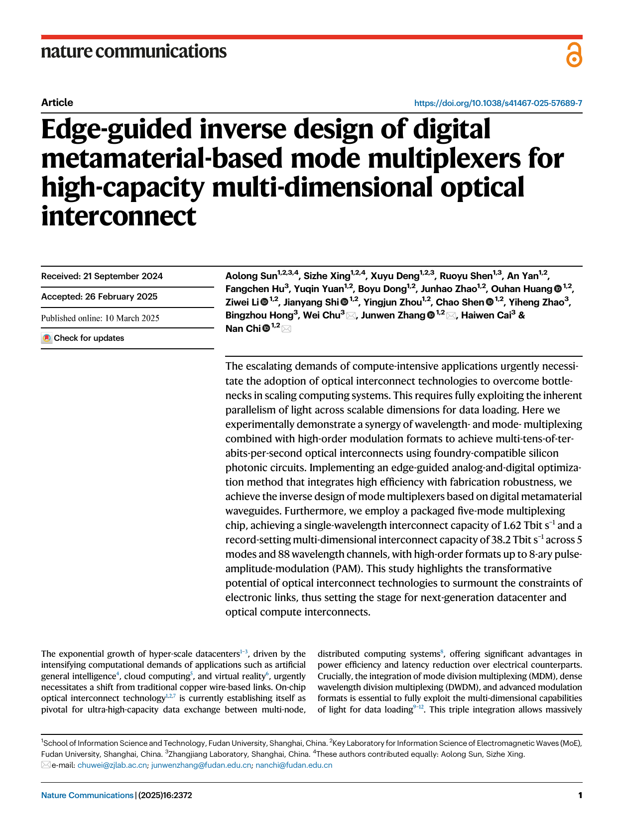
Nature Communications, 16:2372, 2025 · Co-first authorinverse designmode multiplexingoptical interconnectdigital metamaterialssilicon photonics
news
| 2026 · 06 | Co-first-author paper on an inverse-designed silicon six-mode multiplexer for 1.62 Tb/s/λ AI-enhanced MDM interconnect accepted by ECOC 2026, Málaga. |
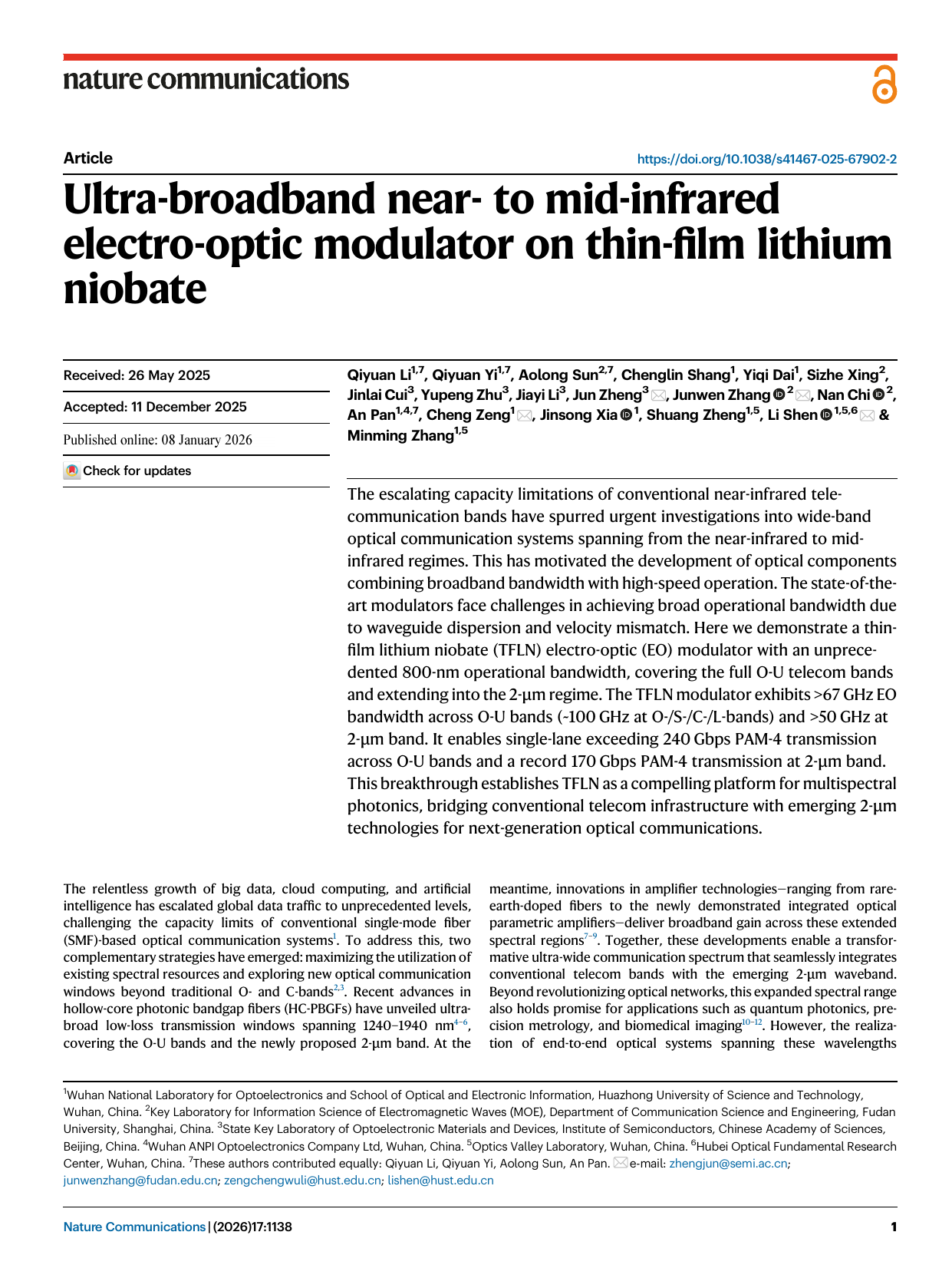
| 2026 · 01 | Co-first-author paper on ultra-broadband near- to mid-IR EO modulator on thin-film lithium niobate accepted by Nature Communications (17:1138). |
| 2025 · 12 | Awarded the NSFC Youth Student Basic Research Project (2026–2027) as principal investigator. |
| 2025 · 11 | Began visiting PhD at A*STAR Institute of Microelectronics (IME), Singapore. |
| 2025 · 11 | Presented at IEEE Photonics Conference (IPC) 2025, Singapore. |
| 2025 · 10 | First-author paper in Photonics Research 13(10) — selected as Editor's Pick. |
| 2025 · 10 | Selected for the CAST Youth Talent Cultivation Program. |
| 2025 · 09 | Awarded the National Scholarship for PhD Students. |
| 2025 · 08 | Special Grand Prize at the China New-Domain New-Quality Innovation Competition. |
| 2025 · 07 | Excellence Award at the National PhD Optics & Photonics Academic League. |
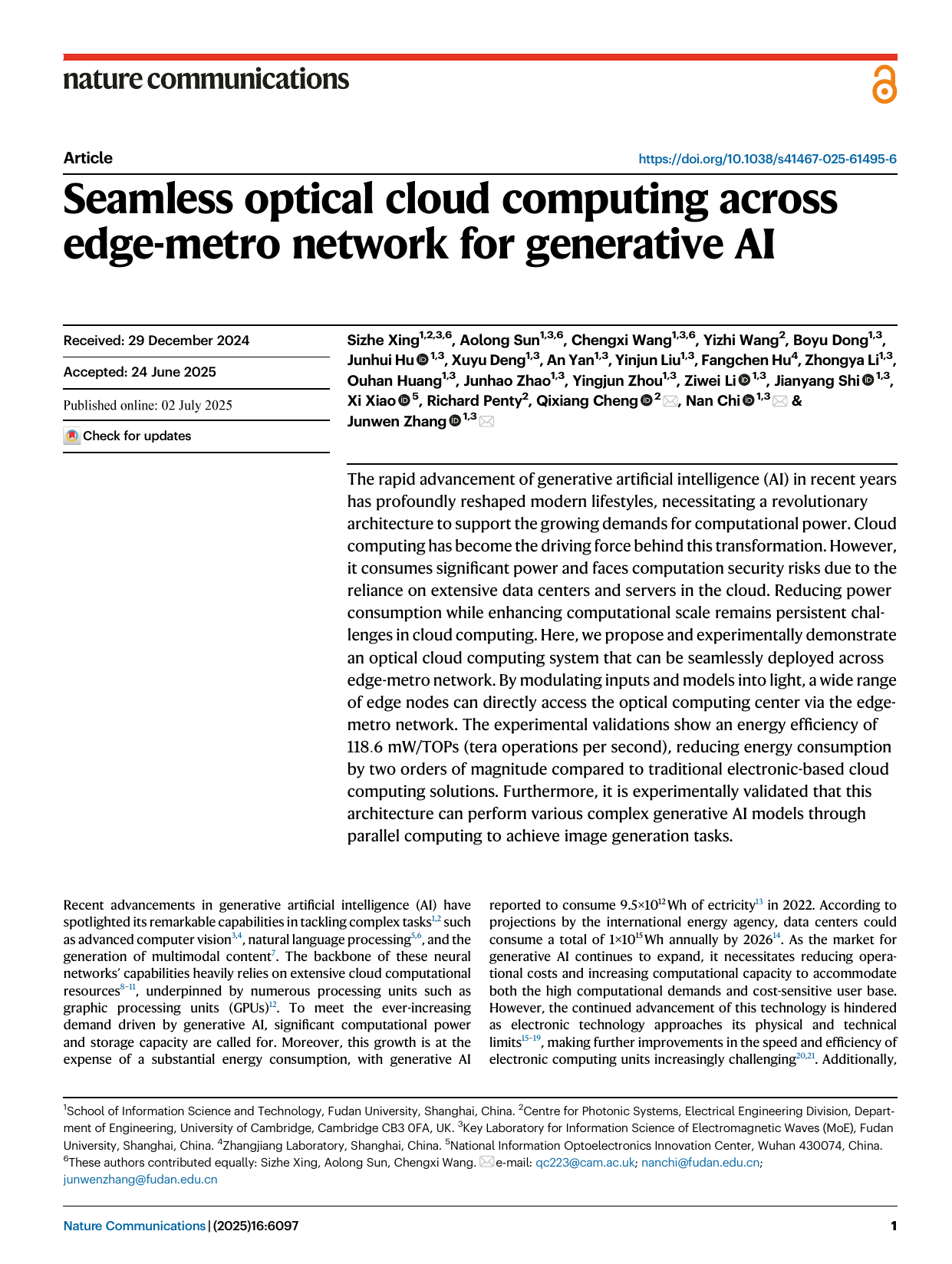
| 2025 · 06 | Co-first-author paper on seamless optical cloud computing for generative AI published in Nature Communications (16:6097). |
| 2025 · 06 | Silver Medal at the China International College Students Innovation Competition (Shanghai). |